

Sapphire Substrate – A-Plane
A-Plane sapphire substrates are useful for hybrid microelectronic applications requiring a uniform dielectric constant and highly insulating characteristics. This orientation can also be used for the growth of high Tc superconductors. The availability of Angstrom level surface finishes allows for fine line interconnects of hybrid modules.
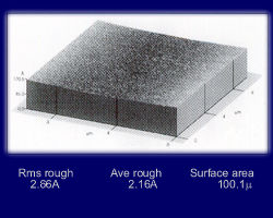
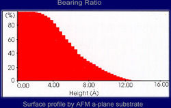
Standard Specification
| Material | Czochralski grown sapphire (>=99.995% High Purity monocrystalline Al2O3). | |
| Surface Orientation | A-Plane (1 1 -2 0) surface orientation, also called 90-degrees. Surface oriented within 0.3-degrees. Other offcuts are available. | |
| Crystallinity | No visual evidence of slips, twins, lineage or fractures | |
| Dimensions | Outer Diameter | 50.8mm ± 0.1mm, 76.2mm ± 0.25mm, 100.0mm ± 0.4mm 150.0mm ± 0.5mm |
| Thickness | 500μm ± 10μm, 430μm ± 10μm, 330μm ± 15μm | |
| Surface Flatness | <25μm, depending on thickness | |
| Surface Bow | <25μm, depending on thickness | |
| Surface Taper | <25μm, depending on thickness | |
| Primary Flat Length | 16mm ± 1mm, 22mm ± 1mm, 32.5mm ± 1mm | |
| Primary Flat Location | Parallel to the C-axis <0 0 0 1>, within 0.2 ° | |
| Edges | The edges of the substrates have a ground finish | |
| Edge Chips | Edge defects in general will not exceed those stated in SEMI M3-91 | |
| Frontside Surface Finish | A smooth, polished surface finish suitable for epitaxy. No visible scratches, pits, dimples or contamination allowed. Ra typically < 0.20nm | |
| Backside Surface Finish | Depends on whether wafer is single side polished or double side polished. SSP: Fine ground, Ra typically 0.4 to 1.5μm. DSP: Polished | |
| Note | Other wafers orientations are available, including R-plane (1 -1 0 2), C-plane (0 0 0 1) and M-plane (1 -1 0 0) | |
The data above is representative only, with a combination of data from our suppliers, and should not be considered absolute or warrantable. Specifications will be in given in our quotations and additional information is available on request. For a quotation please do not hesitate to contact us with your specific requirements.