

Saw Wafers
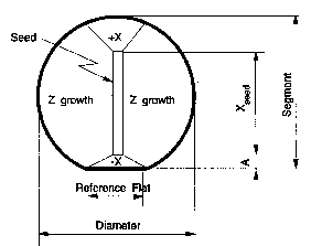
Outline drawing
Single crystal cultured quartz substrate wafer is most commonly specified as 3″ or 100 mm with a reference flat. The wafers are Y-cut with rotations specified between about 32° and 42.75° around the X-axis. A high quality, low damage surface is prepared on one major (propagating) surface by polishing.
The back side is usually lapped to a rough finish to attenuate unwanted vibration modes.
Ex-stock delivery for standard 4″ wafer angles : 32°, 34°, 36°, 37°30′, 38° and 40°.
Typical Specifications
Physical Dimensions
| Description | Units | Tolerance | Range |
|---|---|---|---|
| Diameter | mm | ± 0.1 | 76.2 ~ 100.0 |
| Thickness | mm | ± 0.01 | 0.35 – 0.50 |
| Total thickness variation | mm | maximum | 4.00 |
| Orientation of propagating surface – around X-axis | arc minute | ± 6 | Customer specified |
| Orientation of propagating surface – around Z’-axis | arc minute | ± 15 | 0.00 |
| Reference flat width | mm | ± 3 | |
| Reference flat orientation (xxxx to Y’-axis) | arc minute | ± 6 | 0 |
| Segment | mm | nominal | 74.7 / 98.5 |
| Xseed | mm | minimum | 76 |
| A | mm | maximum | 2 / 5 |
| Centricity of seed | mm | within central 5 |
Seed-free wafers are also available in any of the above dimensions and angles.
Surface Characteristics
| Description | Units | Tolerance | Range | |
|---|---|---|---|---|
| Roughness | Rrms – Propagating surface | nm | maximum | 0.6 |
| Ra – Back side | nm | ±50 | 250 | |
| Bow | µm | maximum | 40 | |
| Scratch length | µm | maximum | 10 | |
| Dig diameter | µm | maximum | 2 | |
| Observable flaws | count | maximum | 2 | |
| Pin holes (at the seed) | count | maximum | 0 | |
| Dimensions of chips | within 1.5mm of edge | mm | maximum | 0.5 |
| on the circular segment of the reference flat | mm | maximum | 0.2 | |
| Wafer edge treatment (not including reference flat) | mechanical bevel | |||
| Rrms: Root Mean Square Ra: Average Peak-to-Valley Distances | ||||
Material Properties
| Description | Units | Tolerance | Range | |
|---|---|---|---|---|
| Growth type | Basal (Z) | |||
| Handednes | right or left | |||
| Twins | none | |||
| α – value (3500 cm¹) | α – units | maximum | 0.060 | |
| Inclusions (diameter) | 25 – 75 µm | cm3 | maximum | 5 |
| 75 – 100 µm | cm3 | maximum | 4 | |
| >100 µm | cm3 | maximum | 3 | |
| Etch channel density | cm2 | maximum | 300 |
Seed Characteristics
| Seed centricity | Within central 3mm | |
| Non-Z material | +X growth | 2.0 mm maximum |
| -X growth | 2.0 mm maximum |
References
International Electrotechnical Commission Standard, CEI/IEC 758, Second edition, 1993-04.
Institute of Electrical and Electronic Engineers Standard on Piezoelectricity, ANSI/IEEE Std. 176-1987.