

Sapphire Substrate – C-Plane
Basal Plane Sapphire Substrates with one or both surfaces polished are useful for the growth of lll-V and ll-Vl compoounds, such as GaN, for bright blue and green LED and laser diodes. Other applications include mercury cadmium telluride for infrared detector applications.

Standard Specification
| Material | Czochralski grown sapphire (>=99.995% High Purity monocrystalline Al2O3). | |
| Surface Orientation | C-Plane (0001) surface orientation, also called 0-degrees, off M (1-100) 0.2°, 0.3° . Other offcuts available. | |
| Crystallinity | No visual evidence of slips, twins, lineage or fractures | |
| Dimensions | Outer Diameter | 50.8mm ± 0.1mm, 76.2mm ± 0.25mm, 100.0mm ± 0.4mm 150.0mm ± 0.5mm |
| Thickness | 500μm ± 10μm, 430μm ± 10μm, 330μm ± 15μm | |
| Surface Flatness | <25μm, depending on thickness | |
| Surface Bow | <25μm, depending on thickness | |
| Surface Taper | <25μm, depending on thickness | |
| Primary Flat Length | 16mm ± 1mm, 22mm ± 1mm, 32.5mm ± 1mm | |
| Primary Flat Location | Parallel to M-axis, within 0.2 ° | |
| Edges | The edges of the substrates have a ground finish. | |
| Edge Chips | Edge defects in general will not exceed those stated in SEMI M3-91. | |
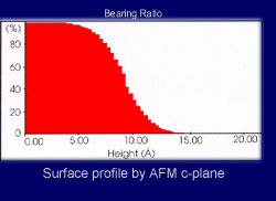
| Frontside Surface Finish | A smooth, polished surface finish suitable for epitaxy. No visible scratches, pits, dimples or contamination allowed. Ra typically < 0.20nm. | |
| Backside Surface Finish | Depends on whether wafer is single side polished or double side polished. SSP: Fine ground, Ra typically 0.4 to 1.5μm. DSP: Polished. | |
| Note | Other wafers orientations are available, including R-plane (1 -1 0 2), A-plane (1 1 -2 0) and M-plane (1 -1 0 0). | |
The data above is representative only, with a combination of data from our suppliers, and should not be considered absolute or warrantable. Specifications will be in given in our quotations and additional information is available on request. For a quotation please do not hesitate to contact us with your specific requirements.